Key Takeaways
- Terafab targets 1 terawatt of AI compute annually, 50x current total global production.
- $25B joint venture between Tesla, SpaceX, and xAI to achieve chip independence.
- 80% of compute output is destined for a constellation of 1 million orbital AI satellites.
- Production facility consolidates design, lithography, fab, packaging, and testing under one roof.
- Two custom chip families: AI5/AI6 for terrestrial robots/cars and D3 for radiation-hardened space use.
- Critics point to massive financial gaps, ASML equipment bottlenecks, and launch cadence challenges.
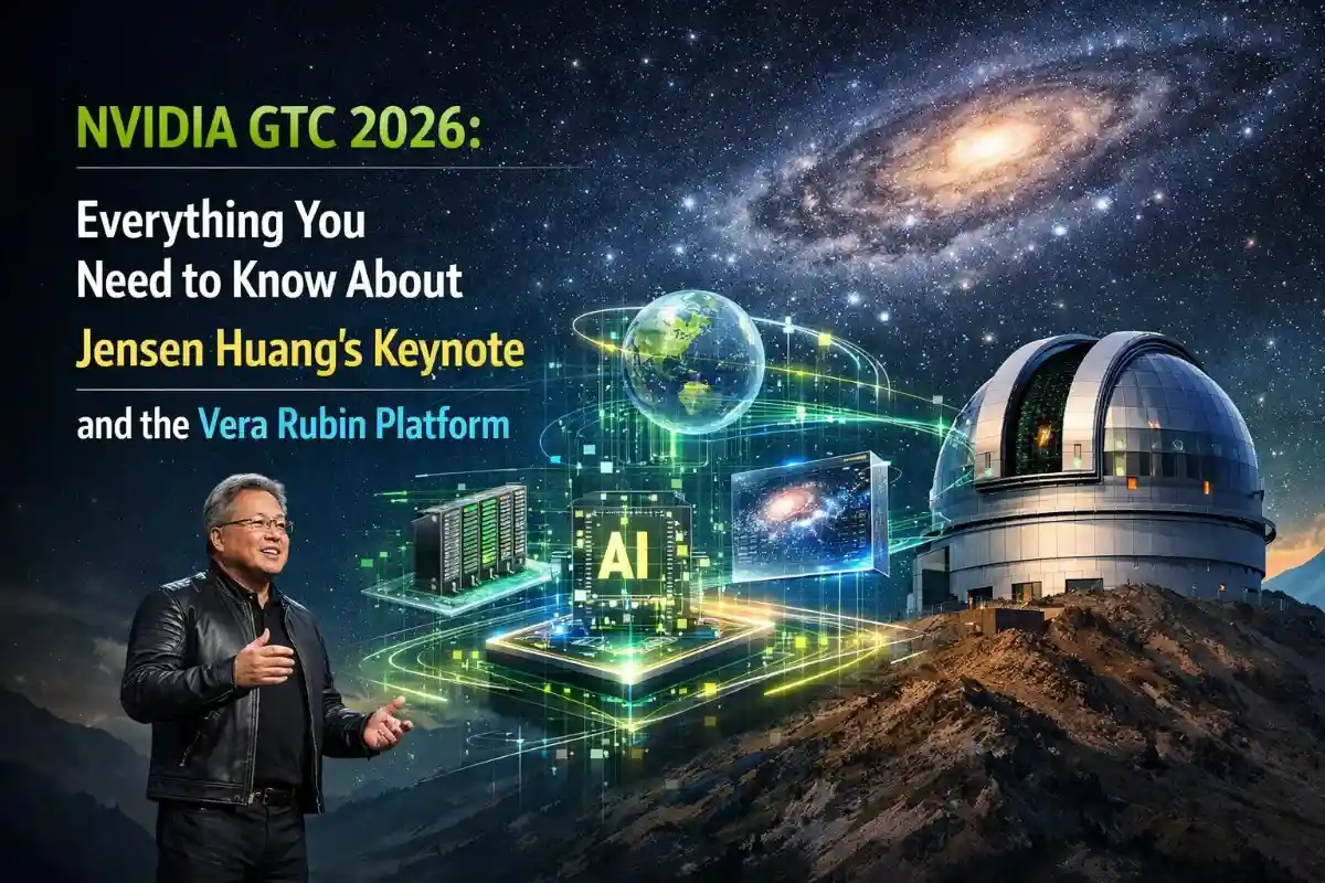
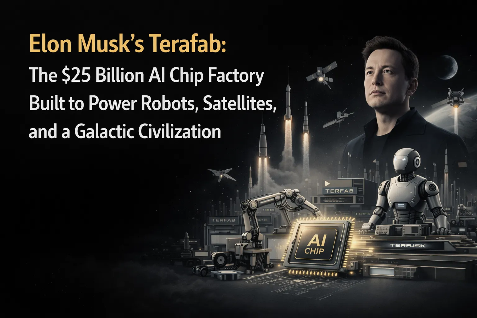
Elon Musk's Terafab: The $25 Billion AI Chip Factory Built to Power Robots, Satellites, and a Galactic Civilization
On March 21, 2026, Elon Musk took the stage at a defunct power plant in Austin, Texas, and announced the most ambitious semiconductor project in history. Terafab, a $25 billion joint venture between Tesla, SpaceX, and xAI, is designed to produce one terawatt of AI computing power per year: 50 times the entire current global output. 80% of those chips are destined not for data centers on Earth, but for one million satellites in orbit. Musk called it "the most epic chip-building exercise in history by far" and described it as "the next step towards becoming a galactic civilization." Here is everything you need to know.
By the Numbers: The Scale of Terafab at a Glance
Terafab's stated goals are so large they require context to understand. Here are all the key numbers from Musk's March 21 announcement, the Wikipedia entry, and subsequent reporting.
| Metric | Figure |
|---|---|
| Announcement date | March 21, 2026: Seaholm Historic Power Plant, Austin, Texas |
| Joint venture partners | Tesla, SpaceX, xAI (SpaceX acquired xAI in February 2026) |
| Estimated cost | $20 to $25 billion (Musk estimate); $35 to $45 billion (Morgan Stanley estimate) |
| Location | North Campus of Giga Texas, Austin (prototype fab); full facility location TBD |
| Target annual compute output | 1 terawatt (1 trillion watts) of AI compute per year |
| Current total global AI chip output | ~20 gigawatts per year |
| Terafab output vs current global output | 50x current total global production |
| Target annual chip production | 100 to 200 billion custom AI and memory chips per year |
| Process technology target | 2-nanometer (2nm): most advanced node entering commercial production |
| Initial wafer starts per month | 100,000 |
| Full capacity wafer starts per month | 1,000,000 (1 million) |
| Two chip families produced | AI5 / AI6 (terrestrial inference) and D3 (space-hardened orbital) |
| Compute output split | 80% orbital (space) / 20% terrestrial (Earth) |
| AI5 small-batch production target | Late 2026 |
| AI5 volume production target | 2027 |
| SpaceX orbital satellite filing (FCC) | License to launch up to 1 million AI data center satellites |
| AI Sat Mini power per satellite | 100 kilowatts of onboard compute per satellite |
| Terafab vs TSMC at full capacity | ~70% of TSMC's total global output |
| Tesla's current global chip suppliers | TSMC, Samsung, Micron (all continuing during Terafab ramp) |
The context for the 1 terawatt target matters enormously. The entire United States generates approximately 0.5 terawatts of electricity annually. Musk is proposing a chip facility that targets more compute output per year than twice the entire U.S. electricity grid. It is not a projection. It is a category jump unlike anything previously announced in semiconductor history.
Why Terafab Exists: The Supply Chain Crisis Behind the Announcement
Terafab did not emerge from nowhere. Musk has been signaling the need for chip independence for over a year, and the logic is straightforward once you understand the scale of what his companies are planning to build.
Tesla, SpaceX, and xAI are already among the largest consumers of advanced AI chips in the world. The demand is only accelerating because the products they are building require extraordinary amounts of compute:
- Tesla wants to produce between 1 billion and 10 billion Optimus humanoid robots annually at full scale, each requiring an AI inference chip to operate
- Tesla's Full Self-Driving system and Cybercab robotaxi fleet require edge-inference processors in every vehicle, at production volumes projected to grow significantly through the late 2020s
- SpaceX is building a constellation of up to one million orbital AI satellites, each requiring a radiation-hardened processor that no current commercial supplier makes at scale
- xAI's Grok model training and inference operations require data center grade compute that xAI has been scaling aggressively since the SpaceX acquisition in February 2026
At Tesla's Q4 2025 earnings call on January 28, 2026, Musk warned investors directly: external chip capacity from TSMC, Samsung, and Micron would hit a ceiling within three to four years that his companies could not grow past. He described the situation without ambiguity at the Terafab launch event: "We're very grateful to our existing supply chain, to Samsung, TSMC, Micron and others, but there's a maximum rate at which they're comfortable expanding. That rate is much less than we would like. And we need the chips, so we're going to build the Terafab."
The fundamental claim that defines the entire Terafab project is that all existing chip fabrication facilities on Earth currently produce only about 2% of the compute that Tesla and SpaceX will eventually need across all their applications. Whether that projection is realistic is a matter of significant debate, addressed in the critics section below. But the chip supply constraint that triggered Terafab is real and is already affecting Tesla's AI and robotics product timelines.
The Corporate Structure: One Man, Three Companies, One Chip Factory
Terafab is a joint venture, but the corporate architecture behind it has changed significantly in the months leading up to the announcement. Understanding the structure helps explain why this project is possible now in a way it was not twelve months ago.
In February 2026, SpaceX completed its acquisition of xAI in an all-stock deal. Elon Musk is now CEO of all three companies simultaneously: Tesla, SpaceX, and xAI. This consolidation under single leadership is what makes Terafab possible as a joint venture rather than a looser partnership. Decisions about chip specifications, production priorities, facility design, and capital allocation can be made without the inter-company negotiation that would normally slow a project of this scale.
The structural logic of the three-way combination for Terafab is:
- Tesla contributes its existing silicon design teams (responsible for AI4, AI5, and AI6 chips), its Austin manufacturing infrastructure at Giga Texas, its experience with vertical integration at scale, and its demand for terrestrial inference chips for vehicles and Optimus robots
- SpaceX contributes its launch infrastructure for the orbital data center constellation, its satellite design capability, its Starlink manufacturing experience, and its demand for D3 space-hardened chips. SpaceX is also the largest single entity contributing to the project's strategic rationale: the orbital constellation cannot exist without a domestic supply of radiation-hardened processors at scale
- xAI contributes model training expertise, AI system design, the Grok model architecture that will run on both terrestrial and orbital hardware, and the software stack that will operate across the combined chip ecosystem
The talent acquisition operation xAI ran in the weeks preceding the Terafab launch reflects this layered strategy. Devendra Singh Chaplot, co-founder of Mistral AI and founding member of Mira Murati's Thinking Machines Lab, joined to work on Grok model training. Andrew Milich and Jason Ginsberg, the engineers who built Cursor to a $2 billion annual revenue run rate, joined to build the product layer. Terafab is the hardware layer. The model layer, the product layer, and the chip layer are all under construction simultaneously. Musk acknowledged at the event that xAI had not been built correctly the first time and that this combined structure is the corrective.
The Facility: What Terafab Actually Builds and How
Terafab's most genuinely novel claim is not its scale. It is its architecture. Every major semiconductor manufacturer in the world operates across multiple geographically distributed facilities. TSMC designs chips in Taiwan, manufactures wafers in multiple fabs, ships them to packaging facilities in different countries, and coordinates testing across a global supply chain. Each transfer between facilities introduces delay, quality risk, and supply chain vulnerability.
Terafab is designed to do all of this under one roof. Musk described the goal as an "incredibly fast recursive loop for improving chip design": the ability to make a chip, test it, revise the mask, and repeat without shipping wafers between sites. This capability does not currently exist anywhere in the semiconductor industry at commercial scale.
The six stages that Terafab consolidates vertically are:
- Chip design: full in-house design capability for both the AI5 terrestrial inference chip and the D3 space chip, integrated with testing feedback from fabrication
- Lithography: the process of using light to etch circuit patterns onto silicon wafers, currently dominated by ASML's extreme ultraviolet machines that cost $380 million each and have a multi-year waiting list
- Fabrication: the physical manufacturing of silicon wafers, targeting 2-nanometer process technology, the most advanced node currently entering commercial production globally
- Memory production: on-site DRAM and storage memory manufacturing, currently dominated by Samsung, SK Hynix, and Micron
- Advanced packaging: the integration of multiple chips into a single package using techniques like chiplets and 3D stacking
- Testing: quality verification of finished chips before deployment, with results feeding directly back into the design-fab cycle
The prototype Advanced Technology Fabrication facility is being built at the North Campus of Giga Texas in Austin, adjacent to Tesla's existing manufacturing base. Texas Governor Greg Abbott was present at the launch event, signaling state government support for the project. The full-scale Terafab facility will be built at a separate location, yet to be determined.
The Two Chips: AI5 for Earth and D3 for Space
Terafab will produce exactly two chip families. Musk was explicit about this structure, saying: "Terafab will technically be two fabs, each making only one chip design." This single-purpose discipline is what makes the rapid design iteration cycle viable: each facility is optimized entirely for one product.
Chip 1: The AI5 and AI6: Edge Inference for Earth
The AI5 is Tesla's fifth-generation AI inference processor, the successor to the AI4 chip currently used in Tesla's Full Self-Driving hardware stack. It is the chip that will power:
- Tesla's Full Self-Driving system in all new vehicle production from 2027 onward
- The Cybercab robotaxi fleet Tesla plans to deploy at scale in 2027
- The Optimus humanoid robot, which Musk projects will be produced at volumes of 1 to 10 billion units annually at full scale
- All autonomous AI decision-making that occurs at the vehicle or robot level, rather than in a cloud data center
The AI5 is the 20% of Terafab's output: the terrestrial slice. Small-batch production of the AI5 is targeted for late 2026 at the prototype Austin facility. Volume production at Terafab is projected for 2027. It is worth noting that Tesla had already delayed the AI5 to mid-2027 before the Terafab announcement, and the AI6 has been pushed back approximately six months due to Samsung's 2nm production timeline slipping. Terafab is positioned as the long-term solution to these supplier-driven delays by eliminating the dependency on Samsung and TSMC for production.
Chip 2: The D3: Space-Hardened Orbital Processor
The D3 is the chip that has no precedent in commercial semiconductor manufacturing. It is a high-power processor specifically engineered to operate in space: in low Earth orbit aboard SpaceX's planned constellation of up to one million AI data center satellites.
Space is a fundamentally different operating environment than any data center on Earth. The D3 must address challenges that no consumer-grade chip can handle:
- Radiation hardening: cosmic radiation and solar particles in low Earth orbit continuously damage conventional silicon in ways that cause bit flips, latch-ups, and permanent degradation. The D3 is designed with radiation-tolerant architecture that prevents these failure modes
- Temperature extremes: satellites in low Earth orbit experience temperature swings from approximately -150°C to +150°C as they move between shadow and direct sunlight every 90 minutes. The D3 must maintain performance across this entire range
- Power efficiency in a constrained environment: each AI Sat Mini carries 100 kilowatts of onboard compute powered by solar panels. The D3 must deliver maximum compute output per watt within that constraint
- Longevity without maintenance: unlike a data center chip that can be replaced during maintenance, an orbital chip must operate reliably for years with no physical servicing possible
The D3 represents 80% of Terafab's total compute output target. The entire orbital constellation logic depends on this chip existing at scale. Without a domestic supply of radiation-hardened, space-optimized processors that can be produced by the hundreds of millions, SpaceX's orbital AI data center vision cannot be realized.
The Galactic Vision: Orbital Data Centers and the Space Computing Bet
The most extraordinary and debated part of the Terafab announcement is not the chip factory itself. It is what those chips are for. Musk's argument that the future of AI computing is in space rather than on the ground is the central thesis of the entire project, and it deserves to be understood on its own terms before being evaluated.
The argument has a straightforward logic:
- The United States generates approximately 0.5 terawatts of total electricity. Running one terawatt of AI compute on Earth would require twice the entire U.S. grid dedicated exclusively to that purpose, an obvious physical impossibility
- In space, solar irradiance is approximately five times greater than at Earth's surface, because there is no atmosphere to absorb or scatter sunlight. A solar panel in orbit generates five times more electricity per square meter than an equivalent panel on the ground
- The vacuum of space eliminates the heat rejection problem that constrains ground-based data centers. On Earth, roughly 40% of a data center's energy consumption goes to cooling. In space, waste heat radiates directly into the vacuum with no active cooling infrastructure required
- Space is effectively free real estate. There is no land acquisition cost, no zoning approval, no grid connection requirement, and no cooling water sourcing challenge
Musk's conclusion from these four facts is that within two to three years, running AI workloads in orbit will be cheaper per watt than running them on the ground. SpaceX has already filed with the FCC for a license to launch up to one million satellites into low Earth orbit. Each satellite in the constellation is currently specified at roughly 170 meters in length with 100 kilowatts of onboard computing power. Collectively, if the full constellation is deployed, these satellites become the largest computing network in human history, powered entirely by solar energy and cooled by the vacuum of space.
Musk has also described longer-term visions beyond the orbital constellation that extend the computing infrastructure to the Moon. He mentioned building an electromagnetic mass driver on the Moon that would use a railgun-like mechanism to launch materials into space without rocket propulsion. "I want to live long enough to see the mass driver on the Moon," he told the Austin audience. On the Moon, with no atmosphere, no weather, and gravity one-sixth of Earth's, the economics of building large-scale solar-powered computing infrastructure are even more favorable than in low Earth orbit.
Tesla's official post on X summarizing the announcement captured the framing in one line: "Announcing TERAFAB: the next step towards becoming a galactic civilization."
"We want to make that real. Not just fiction: to turn science fiction to science fact. That's the glorious, exciting future that I certainly look forward to."
Elon Musk, Terafab launch event, March 21, 2026
What Terafab Means for the AI Industry and NVIDIA
Terafab does not exist in isolation. It is the most dramatic expression of a trend that has been reshaping the semiconductor industry for three years: the shift by hyperscalers and technology giants from buying chips to designing and eventually manufacturing their own.
Apple pioneered this path with its A-series and M-series chips. Amazon followed with Graviton server chips and Trainium AI training chips. Google built its Tensor Processing Units. Microsoft has its Azure Maia AI chips. Meta built its Meta Training and Inference Accelerators. Each of these companies concluded that general-purpose chips from NVIDIA or AMD could not deliver the efficiency, cost, or performance required for their specific workloads at the scale they operate at.
Terafab extends this custom silicon trend to the logical extreme: not just designing custom chips, but manufacturing them. The implications for the semiconductor industry are significant:
- NVIDIA faces a new category of competition. Tesla's AI5 and AI6 chips are specifically optimized for edge inference in vehicles and robots, a market NVIDIA has been targeting with its Drive and Jetson platforms. If Tesla can produce these chips internally at Terafab scale, NVIDIA's automotive AI chip business faces direct displacement
- TSMC and Samsung lose a major customer in the long term. Musk acknowledged his existing suppliers would continue to receive orders during Terafab's ramp-up. But the long-term strategic intent is clear: reduce and eventually eliminate dependence on external foundries for the chip types Terafab produces
- The space computing market creates an entirely new chip category. No major semiconductor company currently produces radiation-hardened AI processors at the volume the D3 will require. If SpaceX's orbital constellation deploys at meaningful scale, Terafab becomes the defining supplier in a market that does not yet meaningfully exist
- Vertical integration becomes the industry's defining strategic question. Terafab is the most aggressive bet yet on the proposition that owning the full stack from chip design through manufacturing through deployment is a durable competitive advantage. Whether it succeeds or fails will be studied as a case study in vertical integration strategy for decades
The Critics: Why Serious Analysts Are Skeptical
The Terafab announcement was met with significant skepticism from industry analysts, semiconductor experts, and financial commentators. Their objections are serious and deserve full representation. Understanding the counterarguments is essential to forming an honest view of what Terafab is likely to achieve and on what timeline.
The Financial Reality Gap
Musk estimated Terafab would cost $20 to $25 billion. Morgan Stanley's semiconductor analysts estimate the real cost of a facility targeting Terafab's stated specifications would be $35 to $45 billion: as much as $20 billion more than Musk's high-end figure. This is not a rounding error. It is a potential 80% cost overrun before a single wafer is started. Tesla's CFO confirmed at the event that the $20 to $25 billion figure is not yet incorporated into Tesla's 2026 capital expenditure plan, which already exceeds $20 billion and is the company's largest ever. Tesla made less than $4 billion in profit in 2025. The financial math requires explanation that has not yet been provided.
The Expertise Problem
Tesla has never manufactured a semiconductor. Chipmaking is categorically different from vehicle manufacturing, battery production, or rocket engineering: the domains where Musk's companies have demonstrated genuine competence. Building a 2nm fabrication facility requires decades of accumulated process knowledge, specialized chemists, physicists, and engineers trained specifically in semiconductor manufacturing, and supply chain relationships with materials suppliers that take years to develop.
The comparison analysts draw most frequently is to Musk's Battery Day announcement in September 2020. That event promised a revolution in battery manufacturing with the 4680 cell, a 50% cost reduction, and production of 10 gigawatt-hours within one year. Five and a half years later, the 4680 program has significantly underdelivered on its original promises. Chipmaking is considered orders of magnitude more complex than battery cell production.
The ASML Bottleneck
Producing chips at 2nm requires extreme ultraviolet (EUV) lithography machines made by a single company in the world: ASML, based in the Netherlands. A single EUV machine costs approximately $380 million and takes two years to manufacture. ASML produces around 50 to 60 machines per year, and every major foundry in the world is on its waiting list. At 100,000 wafer starts per month, Terafab would need multiple EUV machines simply to begin prototype operations. No amount of capital can compress ASML's production timeline, and no technology currently on the market can substitute for EUV at 2nm.
The IP Licensing Challenge
Modern semiconductor manufacturing is built on decades of accumulated intellectual property from hundreds of companies. Chip design tools, process recipes, transistor architectures, memory cell designs, and packaging techniques are all protected by extensive patent portfolios. No company building a new fab from scratch can simply replicate current industry processes. They must either license the relevant IP, develop alternatives from scratch, or acquire companies that hold the necessary patents. Tom's Hardware noted that "no company in their right mind is going to license manufacturing nodes or product technology" to a new entrant that would directly compete with existing foundry customers.
The Space Compute Vision: Bold Math or Fantasy
The Register calculated that putting one terawatt of compute into space, along with the necessary solar power infrastructure, would require launching approximately 10 million tons into space every year. At Starship's current payload capacity of roughly 100 to 200 tons per launch, that requires launching 50,000 to 100,000 Starships per year, which works out to approximately 135 launches per day, or one giant rocket every 10 minutes, every day, indefinitely. SpaceX's current launch cadence is approximately 150 to 200 launches per year across all vehicles. The gap between current capability and the stated vision is not incremental. It is multiple orders of magnitude.
Sam Altman responded to the orbital data center plans directly, calling them "ridiculous" for current AI computing needs in an X post, reflecting a broader view in the AI industry that the timeline for space-based compute to be competitive with terrestrial infrastructure is far longer than Musk suggests.
"Chipmaking is orders of magnitude more complex than battery cell production. The Terafab and orbital data centers may well be the future, but it will take many years to even partially accomplish Musk's promises."
NotebookCheck, Terafab analysis, March 22, 2026
Musk's Track Record: Which Promises Delivered and Which Did Not
Any honest assessment of Terafab must weigh the evidence of Musk's manufacturing execution history. That history is genuinely mixed, which is why the analyst community is divided rather than uniformly skeptical or uniformly enthusiastic.
The cases where Musk's impossible-sounding promises have been delivered:
- SpaceX reusable rockets: the aerospace industry said reusable orbital rockets were not economically viable. SpaceX proved the opposite, created an entirely new commercial launch market, and has made rocket reusability standard practice. The Falcon 9 has completed over 300 successful landings
- Tesla Gigafactories: critics doubted Tesla's ability to build and operate gigascale manufacturing facilities. Tesla has now built six Gigafactories across three continents
- Starlink global internet: dismissed as technically and economically unviable by multiple telecommunications experts. Starlink now has over 6 million subscribers across more than 100 countries and is the leading satellite internet provider globally
- Starship development: after multiple dramatic test failures, SpaceX has reached successful orbital test flights with the largest rocket ever built
The cases where Musk's manufacturing promises significantly missed their stated timelines or targets:
- Full Self-Driving: promised as "one year away" repeatedly from 2016 through 2024. The technology has improved significantly but has not reached the Level 4 or Level 5 autonomy Musk repeatedly projected
- Tesla 4680 battery cell: Battery Day 2020 promised a 50% cost reduction and 10 GWh of production within one year. Tesla's own top battery supplier later said Musk "doesn't know how to make battery cells." The 4680 program is years behind its original targets
- The Hyperloop: announced in 2013 as revolutionizing intercity transportation. No functional Hyperloop system exists anywhere in the world
- Tesla Robotaxi: promised "one million robotaxis on the road by 2020." The Cybercab was unveiled in 2025 and is targeted for commercial deployment in 2027
The pattern from this history is consistent and instructive: Musk's most transformative achievements have been in physics-constrained engineering domains (aerospace, energy storage chemistry, and satellite communications) where, energy storage chemistry, and satellite communications: where the constraints are defined by physical laws rather than manufacturing process complexity. His most significant misses have been in precision manufacturing domains where the constraints are defined by accumulated process knowledge, supply chain relationships, and production scale-up complexity. Chip fabrication is the latter category.
Frequently Asked Questions About Terafab
What is Terafab and who owns it?
Terafab is a $25 billion semiconductor fabrication joint venture between Tesla, SpaceX, and xAI, announced by Elon Musk on March 21, 2026, in Austin, Texas. SpaceX acquired xAI in February 2026, making Musk the CEO of all three companies. Terafab will consolidate chip design, lithography, fabrication, memory production, packaging, and testing under one roof at the North Campus of Giga Texas.
What chips will Terafab produce?
Terafab produces two chip families. The AI5 and AI6 are edge-inference processors for Tesla's Full Self-Driving system, Cybercab robotaxi, and Optimus humanoid robots. The D3 is a radiation-hardened chip designed for operation in space aboard SpaceX's orbital AI satellite constellation. Musk has stated 80% of Terafab's compute goes to space and 20% to terrestrial applications.
How much compute will Terafab produce per year?
Terafab targets one terawatt of AI compute output annually at full capacity: 50 times the entire current global AI chip industry output of approximately 20 gigawatts. Musk's stated long-term target is 100 to 200 billion custom AI and memory chips per year, starting with 100,000 wafer starts per month initially, scaling to 1 million at full capacity.
What are Terafab's orbital data centers?
SpaceX has filed with the FCC to launch up to one million AI data center satellites into low Earth orbit. Each satellite carries 100 kilowatts of onboard compute powered by solar energy. The D3 chips from Terafab are the enabling technology. Musk projects that within two to three years, running AI workloads in orbit will be cheaper per watt than on the ground, because solar irradiance in space is five times higher and the vacuum eliminates heat rejection costs.
How does Terafab compare to TSMC?
At full capacity, Terafab would reach roughly 70% of TSMC's total global output. However, TSMC spent decades and hundreds of billions building manufacturing expertise that Tesla has never had. Terafab targets 2nm process technology that TSMC is only now beginning to ramp. Morgan Stanley estimates the true cost could be $35 to $45 billion, far beyond Musk's $25 billion estimate.
What is Musk's galactic civilization vision with Terafab?
Musk described Terafab as "the next step towards becoming a galactic civilization." His vision is that Terafab chips power billions of Optimus robots and Tesla autonomous vehicles on Earth, while D3 chips power one million orbital AI satellites. Those satellites become history's largest computing network, powered by unlimited solar energy, and supply the computing infrastructure for SpaceX's mission of making humanity multi-planetary, starting with the Moon and eventually Mars.
Final Thoughts: The Most Ambitious Chip Project in History: Whether It Works or Not
The Terafab announcement is going to be debated for years. Either Elon Musk will build the largest semiconductor facility in history, power a million orbital AI satellites with chips no one else can make, and lay the physical foundation for a civilization that extends beyond Earth: or he will not, and Terafab will join the list of ambitious Musk announcements that delivered significantly less than promised on the timelines stated.
The honest position, supported by both the track record and the technical analysis, is that the truth will fall somewhere between these outcomes. Terafab will be built, because the chip supply constraint that motivated it is real and Musk's companies have genuine demand that their current suppliers cannot meet. But it will not produce one terawatt of compute by 2028. The 2nm process technology will take longer to develop than announced. The cost will significantly exceed the $25 billion estimate. And the orbital data center constellation will operate on a timeline measured in decades, not the two to three years Musk suggested.
What Terafab represents regardless of its specific outcome is a genuine inflection point. It is the moment that the AI hardware infrastructure race extended from a competition among existing semiconductor companies and cloud providers to include a new class of vertically integrated AI infrastructure builders who are not content to buy chips from anyone. The fact that the most audacious version of this vision comes from Elon Musk, whose track record includes both the most improbable engineering achievements of the past twenty years and some of the most spectacular manufacturing delays, makes Terafab exactly the kind of story that defines an era regardless of how it ends.
In Austin, Texas, at a defunct power plant, with light beams shooting into the sky and a governor sitting in the audience, Musk said: "The most epic chip-building exercise in history by far." He has said things like that before. Sometimes he was right.
💡 Strategic Insight
This isn't just technical knowledge, it's the kind of engineering thinking that separates production systems from toy projects. Apply these patterns to reduce costs, improve reliability, and ship faster.
Frequently Asked Questions
Terafab is a $25 billion semiconductor fabrication joint venture between Tesla, SpaceX, and xAI, announced by Elon Musk on March 21, 2026. It is designed to be the world's largest vertically integrated AI chip facility.
Terafab will produce two families of chips: the AI5 and AI6 for edge-inference (Tesla vehicles and Optimus robots), and the D3, a high-power radiation-hardened chip for SpaceX's orbital AI satellite constellation.
Terafab is targeting one terawatt of AI compute output per year, which is approximately 50 times the current total global output of the AI chip industry.
SpaceX plans to launch up to one million AI satellites into low Earth orbit. These satellites carry 100 kilowatts of compute power, utilizing the higher solar irradiance and vacuum cooling of space.
At full capacity, Terafab would produce roughly 70% of TSMC's total global output, targeting the advanced 2-nanometer process technology.
Tagged with
TL;DR
- Terafab targets 1 terawatt of AI compute annually, 50x current total global production.
- $25B joint venture between Tesla, SpaceX, and xAI to achieve chip independence.
- 80% of compute output is destined for a constellation of 1 million orbital AI satellites.
- Production facility consolidates design, lithography, fab, packaging, and testing under one roof.
- Two custom chip families: AI5/AI6 for terrestrial robots/cars and D3 for radiation-hardened space use.
- Critics point to massive financial gaps, ASML equipment bottlenecks, and launch cadence challenges.
Need help implementing this?
I help teams architect scalable systems, build AI-powered applications, and ship production-ready software.
Written by
Gaurav Garg
Full Stack & AI Developer · Building scalable systems
I write engineering breakdowns of major tech events, architecture deep dives, and practical guides based on real production experience. Every post is built from code, not theory.
7+
Articles
5+
Yrs Exp.
500+
Readers
Get tech breakdowns before everyone else
Engineering insights on AI, cloud, and modern architecture, delivered when it matters. No spam.
Join 500+ engineers. Unsubscribe anytime.